Significant progress has been made in the preparation of new two-dimensional stanene and the study of its crystalline structure, phonon properties, and electronic structures through the joint efforts of the Surface Physics and Quantum Materials Team of the School of Physics of Beihang University and the Beihang-UOW Joint Center, the team of Zhao Jijun of Dalian University of Technology, and the team of Wang Jia’ou of the Institute of High Energy Physics of the Chinese Academy of Sciences. A monolayer of stanene with warping structure is successfully prepared by utilizing molecular beam epitaxial growth. Combined with first-principles calculations, meticulous research has been conducted on the structural evolution of the “alloying and de-alloying” process of tin atoms on Au(111) single crystal, and on the modulation of lattice internal stress on the vibrational phonon modes of two-dimensional stanene. On March 18, relevant research results were published online inThe Journal of Physical Chemistry Letters(DOI: 10.1021/acs.jpclett.9b00348).
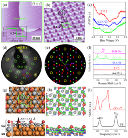
Stanene is an ideal two-dimensional topological insulator with a large energy gap. It is expected to realize the room-temperature quantum spin Hall effect, which is of great significance in the application of spin electronic devices. After repeated trial and error in the last two years, the joint team has successfully used low-temperature molecular beam epitaxy technique to prepare a monolayer stanene "R3×R7-stanene" with a superlattice structure on Au(111) single crystals ( see Fig. a & b). Interestingly, before the formation of two-dimensional stanene, due to the interaction between tin atoms with the gold atoms on the substrate, two two-dimensional structure phases, 2×2(SnAu3) and (R3×R3) R30° (SnAu2), are sequentially formed as the coverage increases. Finally, the R3×R7 stanene (see Fig. d & e) with complex diffraction spots appears after the process of de-alloying. The scanning tunneling spectrum (STS) shows that de-alloyed two-dimensional stanene still has an electronic structure with certain metallicity (see Fig. c). Compared with alloy phase Raman spectroscopy, stanene’s unique vibration modes of in-plane E2g and out-of-plane oTO (see Fig. f) fully demonstrate its two-dimensional property. Combined with the atomic model calculated by the first principles (see Fig. g), it is also found that the R3×R7 stanene superlattice is rather consistent with 1×2 FS stanene. The warping structure and the interaction on the substrate result in up to 8.73% tensile stress in the lattice. Under the effect of such a large tensile stress, the E2g vibration peak of R3×R7 stanene significantly shows a redshift compared to FS stanene (see Fig. i), corresponding to a significant enhancement of the electron-phonon coupling (EPC) intensity. Therefore, this work clarifies that the vibration mode, EPC intensity and electronic structure of stanene can be modulated by stress, which provides a possible regulation for the application of stanene in fields such as spin electronic devices.
The first author of this thesis is Liu Yani, a doctoral student of Beihang-UOW Joint Center’s “Joint Dual Doctoral Training Program”. Since the center’s establishment in 2014, it has made fruitful cooperative achievements through the joint efforts of teachers and students and the support of the Chinese and Australian universities. The “Joint Dual Doctoral Training Program” provides a rare opportunity and a broad platform for the cultivation of high-quality talents. In the future, the two universities will continue to train doctoral students together and conduct more extensive scientific research exchanges on the top of it.

Fig. a & b: Large-scale and atomic-scale topography of two-dimensional stanene
Fig. c: STS spectrum
Fig. d & e: Tin experiment and simulating LEED diagram
Fig. f: Raman spectroscopy
Fig. g: Atomic structure model
Fig. h: Charge differential density map
Fig. i: Vibration state density map